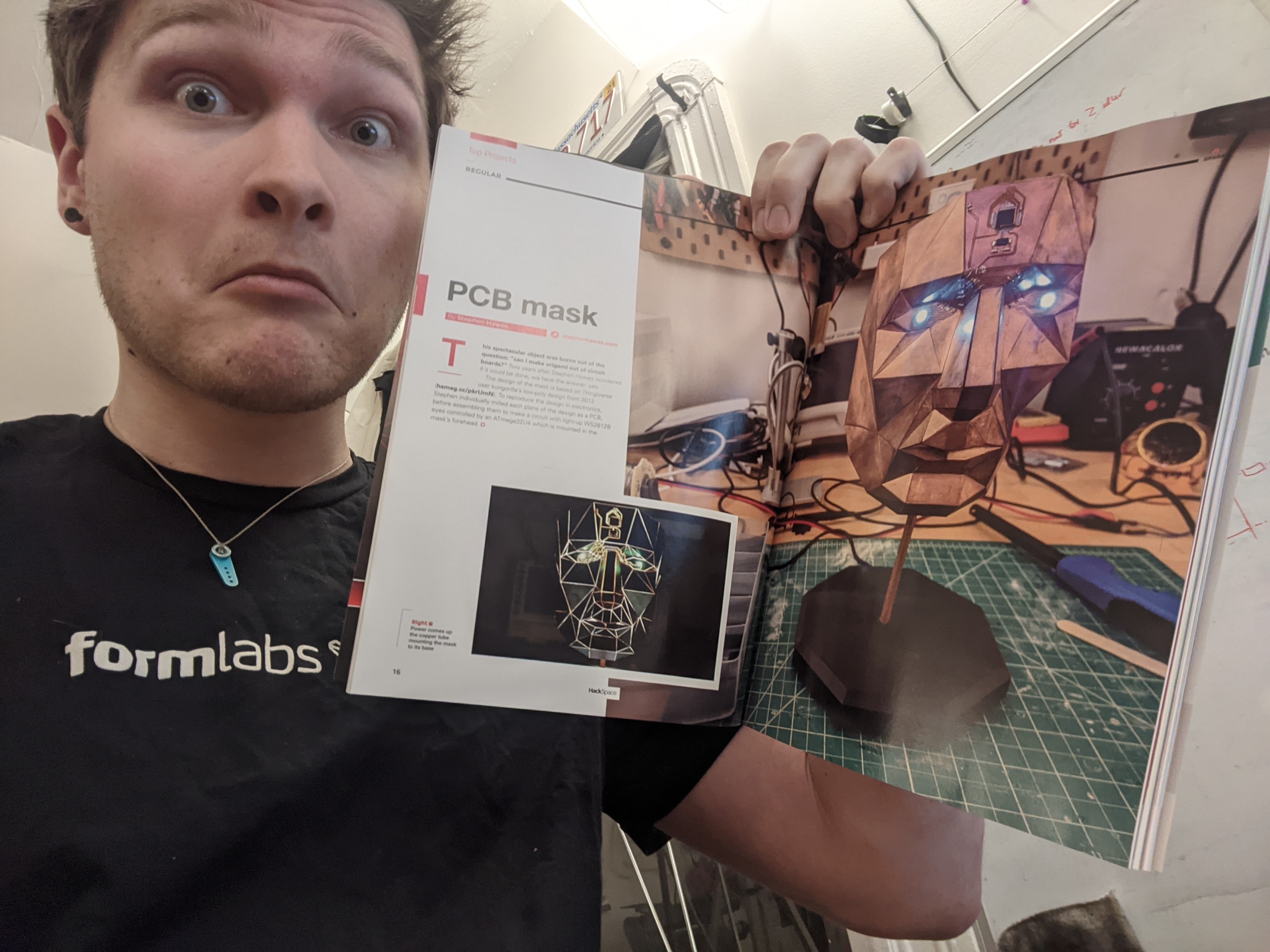
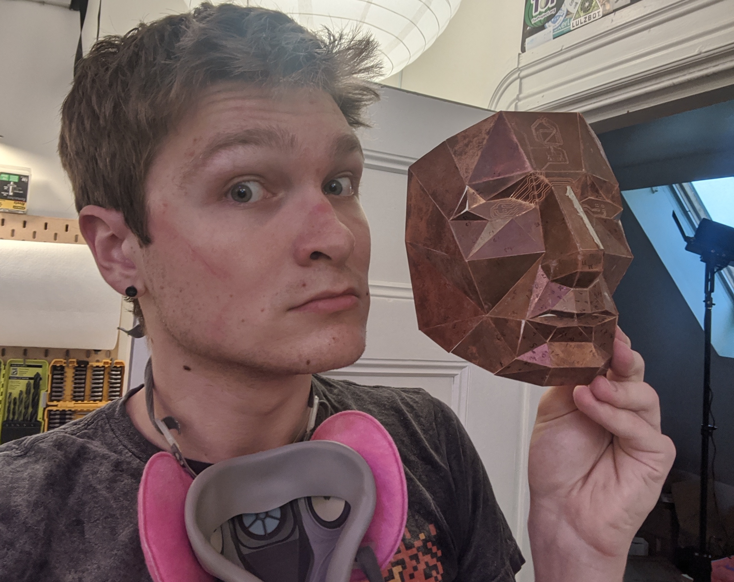
PCB Mask
Pepakura Designer is a digital unwrapper. You give it a mesh, and it effectively unwraps it into a series of flat, foldable shapes.
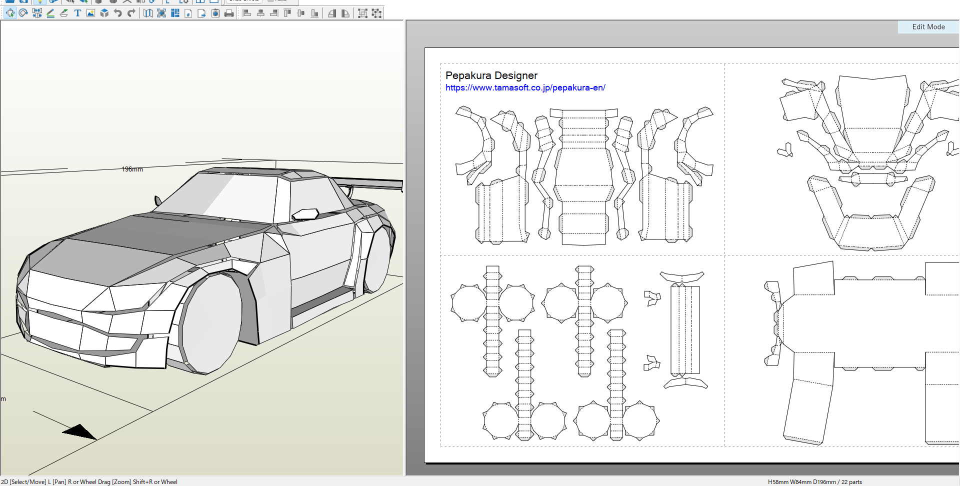
It’s mainly intended to be used for papercraft. Folks with a low-poly 3D model can make a very large, potentially detailed shape using only paper. Plus they can have color very easily, given that the pieces are being printed anyway.
I wondered if the same process could be done with PCBs.
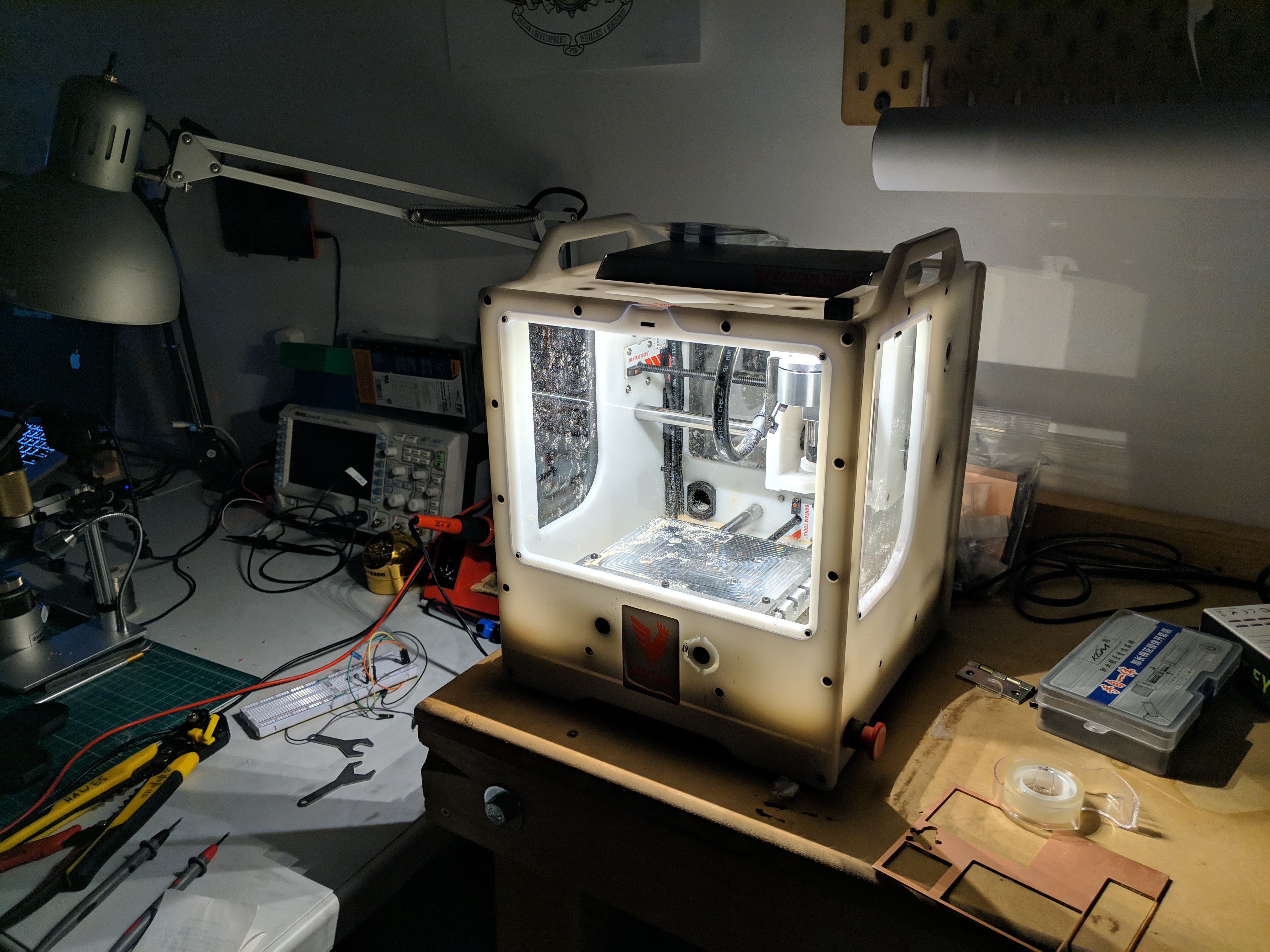
Bantam Tools generously loaned me a PCB Mill as part of their Remote Resident program, so I used Pepakura to unwrap a popular STL of a face, edit it in KiCad, and mill them out.
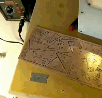
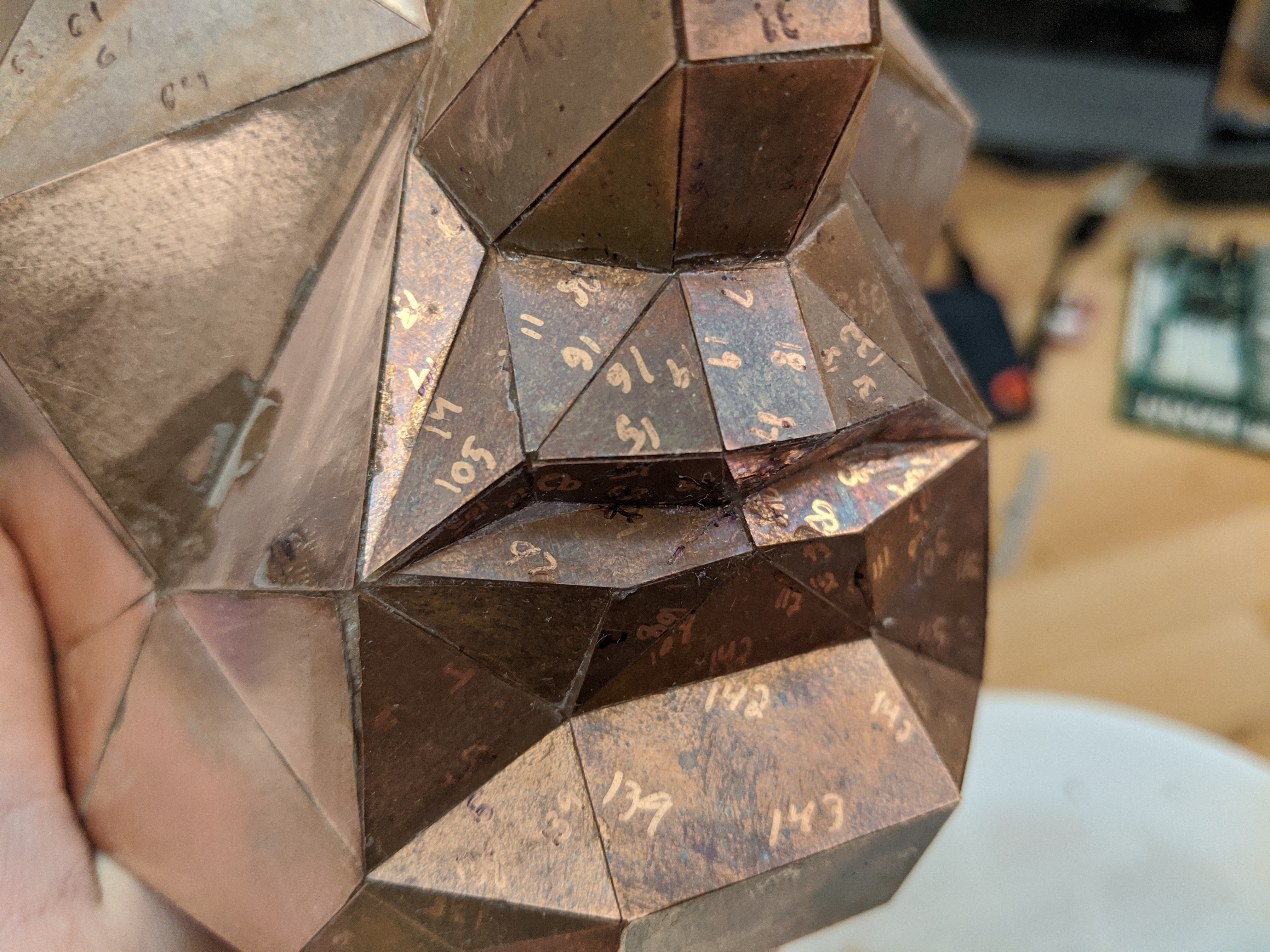
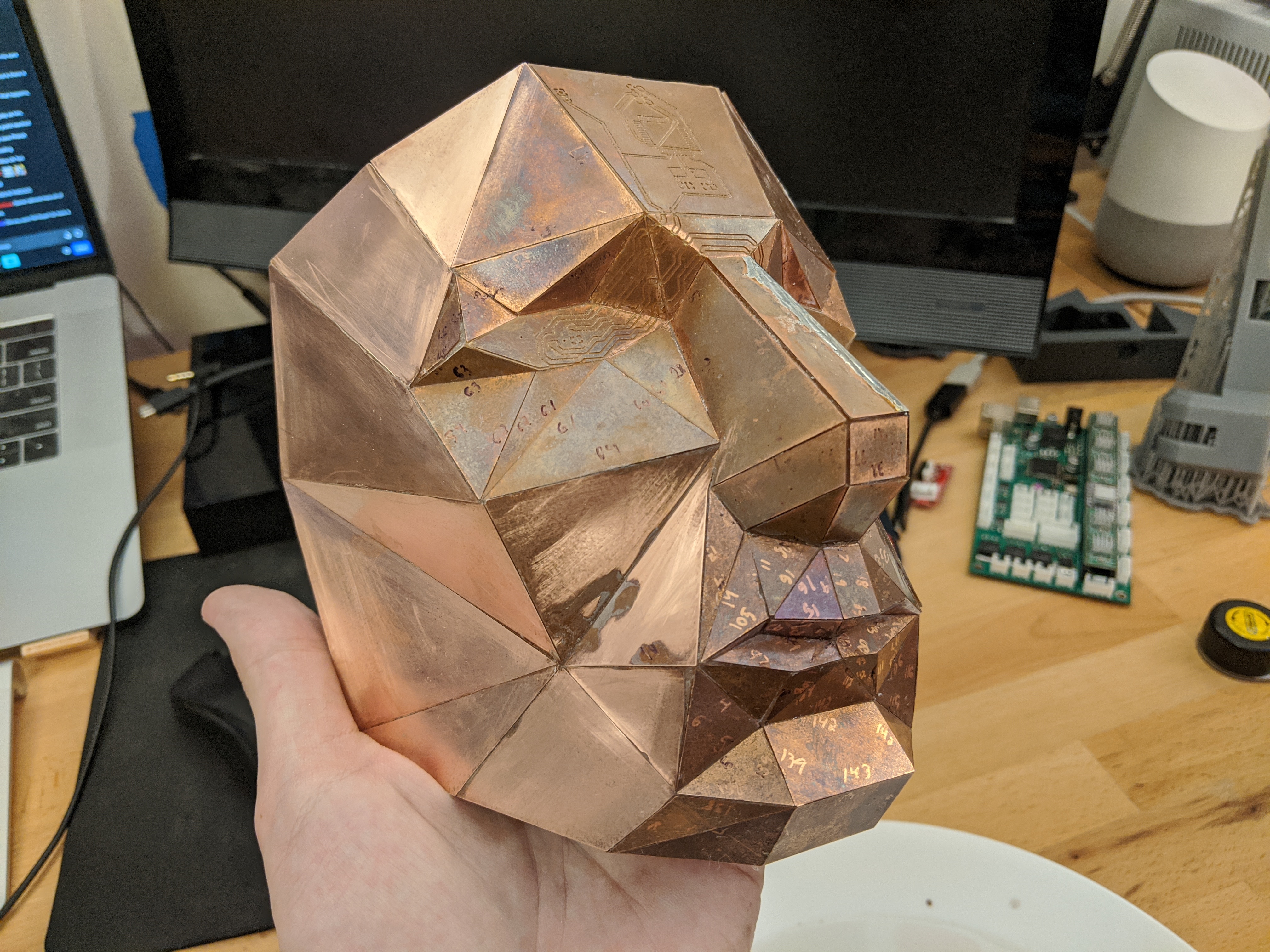
I made sure to number every edge to make sure I would be able to match them up later.
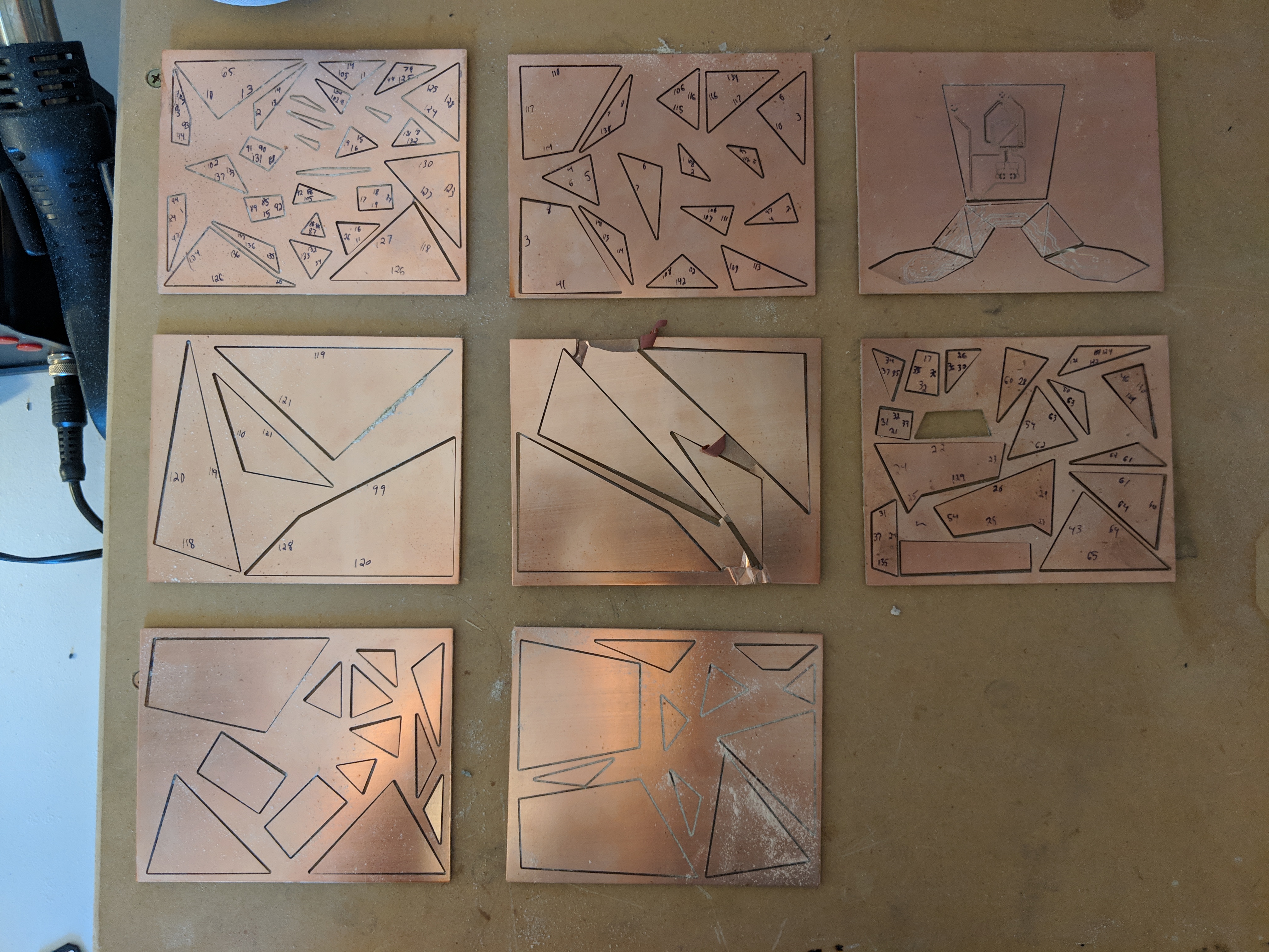
It turns out, this was the easy part. Pepakura is designed to unwrap for a medium that has effectively zero thickness. However, the PCBs I used for this project were the standard 1.6mm PCB thickness.
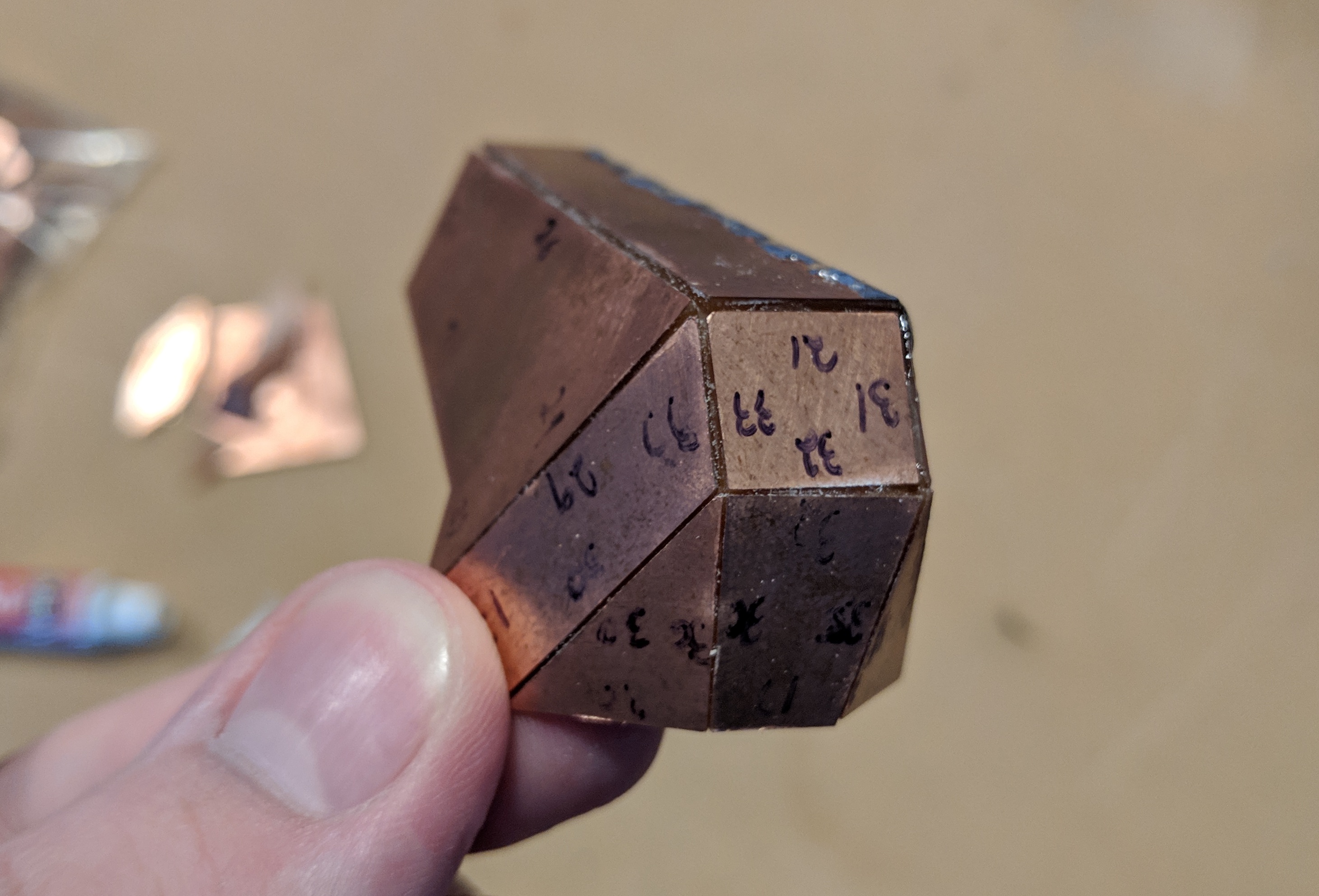
This means I had to manually sand a chamfer into each and every piece.
Thus ensued an 18 month span of sanding FR4 on nights and weekends. Most of the pieces were quite tiny, so the main bottleneck was my hands getting tired holding these small parts and trying to grind them down.
Once I had a handful of parts sanded, I began glueing them together, starting from the nose.
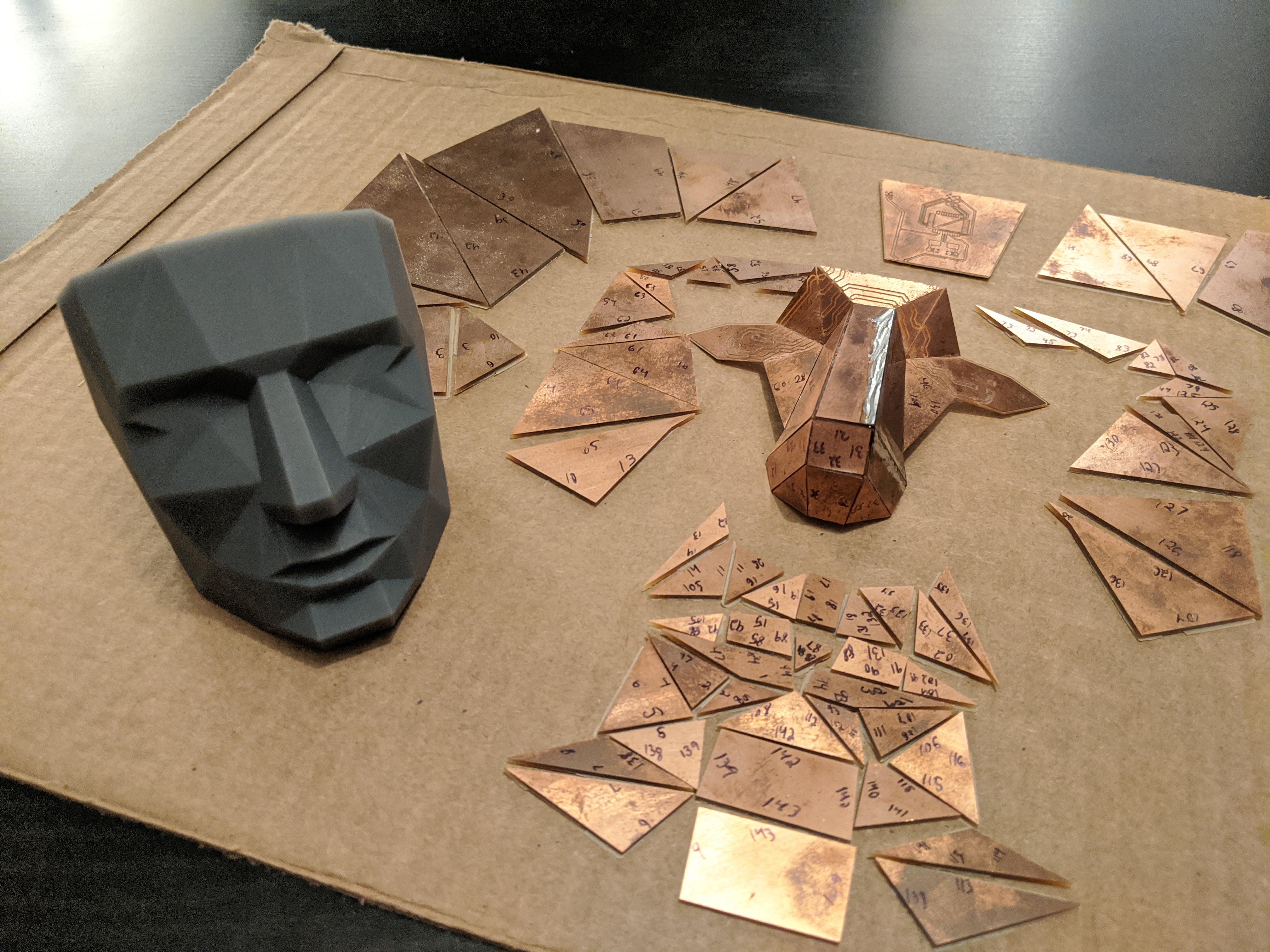
I tried to keep the relevant pieces oriented correctly as I worked, along with constantly referencing a print of the model to help me make sure my angles were correct.
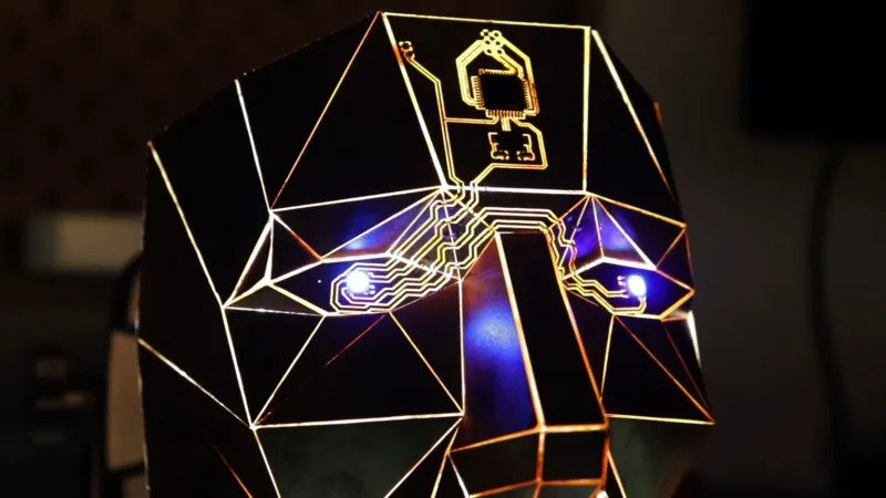
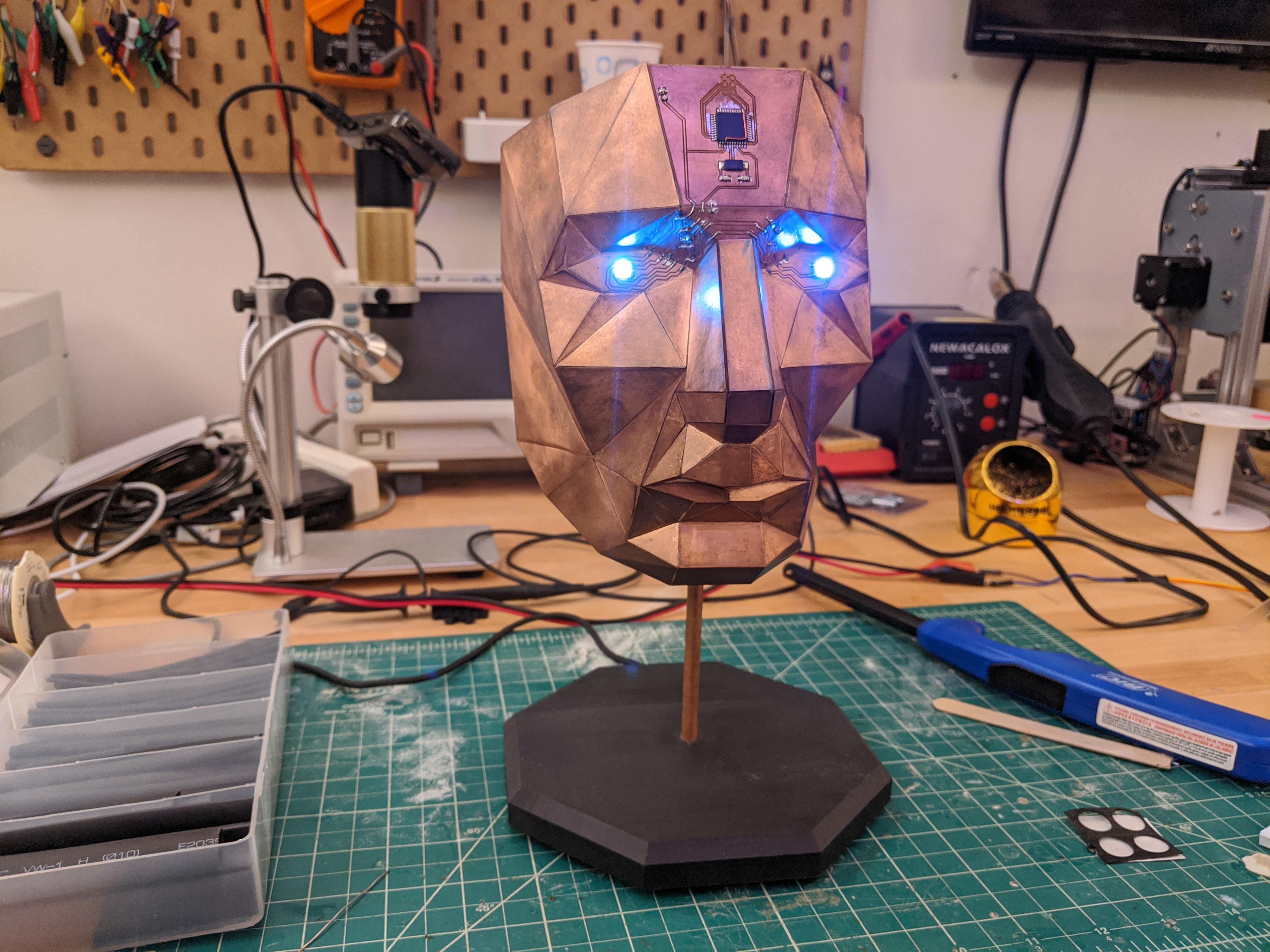
While I was editing the panels in KiCad, I decided to actually add traces traversing between the different PCBs. While a sculpture would be cool in and of itself, I thought it would be signficantly cooler to have an actual circuit wrap around the topology.
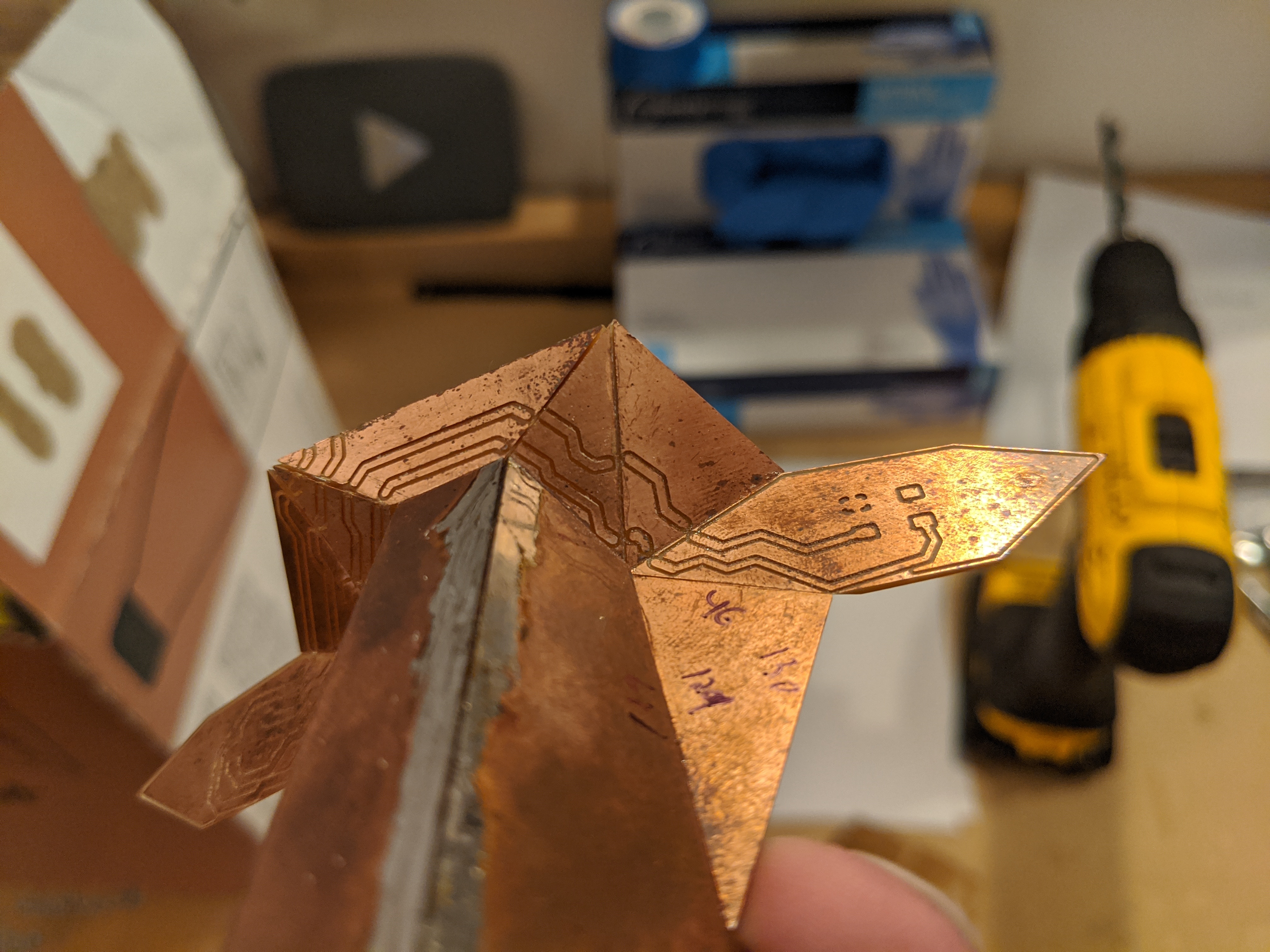
I settled on a simple microcontroller on the forehead, and a few WS2812B LEDs in the eyes.
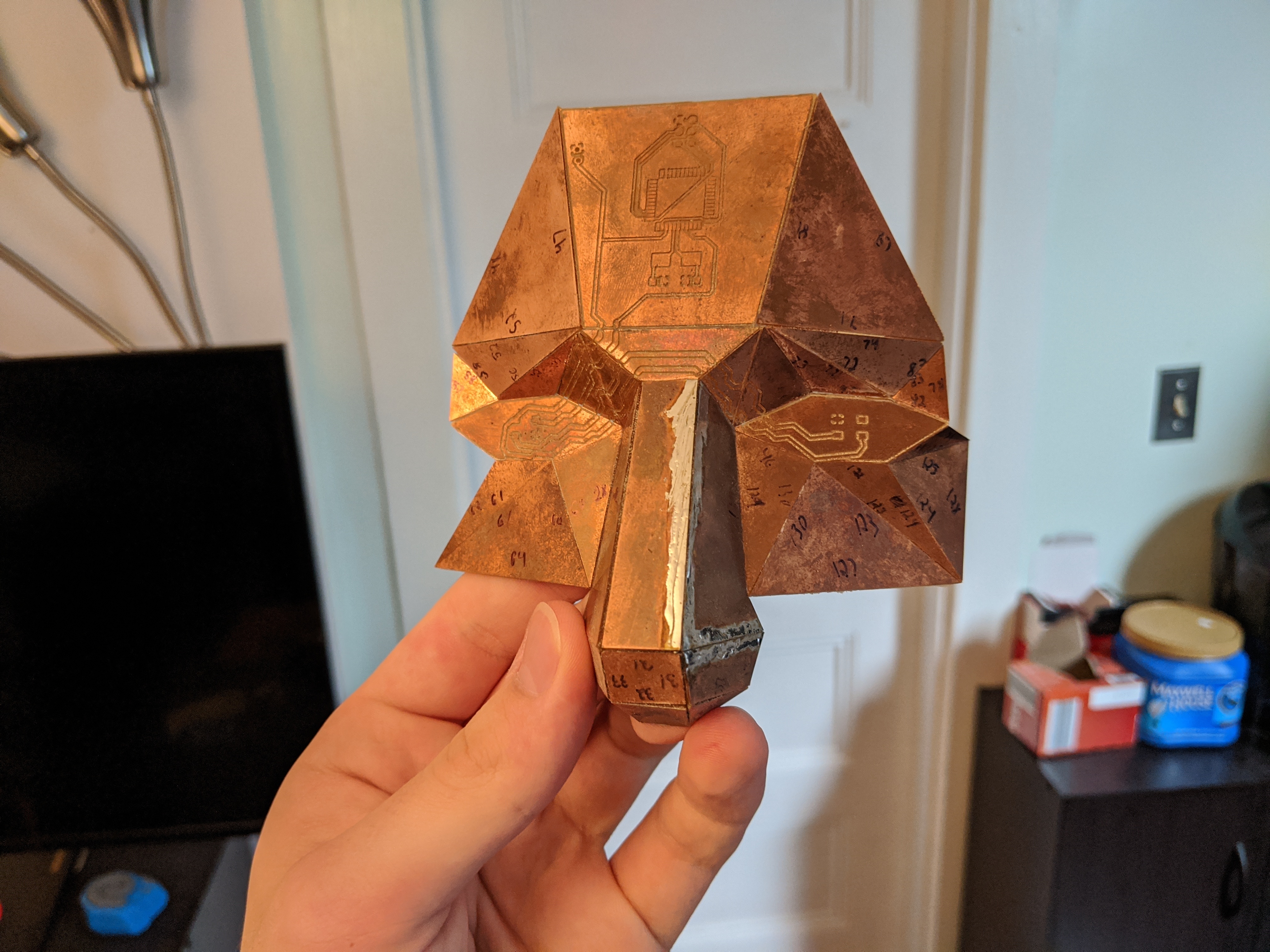
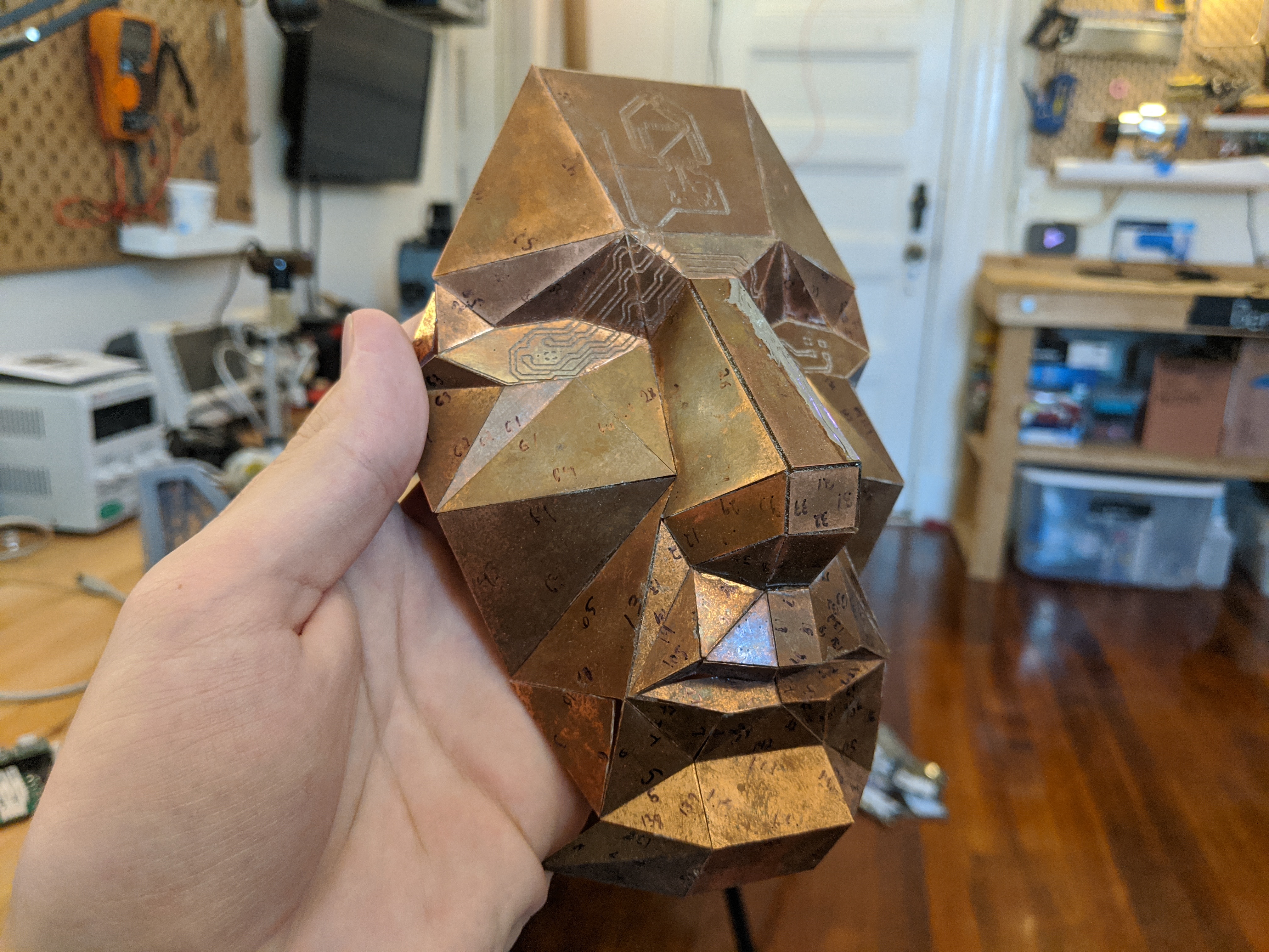
After many months of sanding and glueing, the face was fully assembled.
At this point, it had been an entire year and a half since I milled out the panels, so they needed a good sanding to remove the patina, fingerprints, and leftover sharpie marks.
After soldering on the components, wiping it down with IPA, and giving it a clear coat, I mounted it to a printed base and tossed some firmware onto it.
This was a tremendously satisfying project. I absolutely love the final result, and would love to try to do the same type of thing with a more complicated circuit, ideally with the fact that the PCB is an odd shape actually providing some functionality.